
My Trade Secrets to making quality Printed
Circuit Boards (Updated!)
Release 2.4 Apr 15, 2014
Urgent update! As of late 2013 and early 2014 I have found it virtually impossible to obtain Kodalith negatives from printers anymore. Because of this, the instructions that follow are almost useless. Since I don't give up easily I have had to rely on making my own negative films. The history and instructions on making negative films are at this new page: FilmHistory.
Updated! Some of the chemicals used in the KPR method are no longer available due to potential health hazards. I have now transitioned to the Dry Film/water soluble developing method. Changes in this method are in green, primarily sections 4 and 7.
Note: Kepro had gone out of business in June 2003. Many of the Kepro products are being carried by Camcon Chemical
Please visit the web page Thru-holes for an explanation on how to make low cost thru hole connections.
Note: There are two systems in developing resist images for making circuit boards. Positive and negative process. The method described here is the negative image process. With pre-sensitized negative image process, Kepro sensitized boards provided the best overall value to quality ratio. Since Kepro has ceased operations, the only problem is to locate another board supplier that can provide the pre-sensitized material or sensitize them yourself. The process is explained in this web page but the sensitizing chemical is very expensive and sold only in large quantities whereas you will need only a small amount to sensitize many boards.
Over the years I have seen many published articles and stories on how to make good printed circuit boards. Of course there are many ways to make boards and everyone has their favorite. In producing quality boards one must keep in mind cost, consistency, accuracy, economics, available tools, chemicals and equipment. After over thirty five years of making printed circuit boards by hand, probably over 6000 different patterns, both single and double sided, with almost no failures, I have decided to share some of my "secrets" in making good circuit boards.
There has been much talk of using a copy machine or laser printer and to iron on the toner as resist. I have seen and experienced limited results (pinholes), creeping, and questionable resolution with this method. My method insures excellent repeatability and quality. The negatives can be used over and over again and will definitely outlast your lifetime.
It is not unusual for me to come up with a circuit idea in the morning and by early afternoon having a completely functioning unit assembled and installed in a box!
This commercial unit is a "home brew"
There are 9 steps to my process.
Lay out the circuit in a CAD program..
Print the circuit pattern to paper at 2X (two times) the real size.
Reduce the positive to a negative 1X (one times) on photographic Ortho film.
Contact expose the board using the film and sensitized board.
Develop the board.
Etch the board.
Remove the resist.
Drill the board and shear to size.
Tin plate the board. (Optional)
This may seem like a lot, but its quick enough and the results are excellent.
1. Coming up with the layout. Back in the 70's and before, draftsmen used tape and donut pads on a sheet of acrylic, mylar, clearprint, or vellum. Everything was done by hand with an Xacto knife and a light table. I have spent many thousands of hours on a light table making boards as large as 18" X 36" double sided and 2X (2 times).
A question often asked is why 2 times the size? It makes for working on small circuits with small tracks a lot easier. Also when an artwork is reduced, resolution (sharpness) is increased, and slight errors in dimensions are halved. Sometimes we even worked 4X but 2X was the standard. I have never laid out a 1X board.
Obviously the drawbacks using tape and pads are considerable. Repeating patterns, moving, or reworking a circuit layout was tedious. The tape and pads had a very limited life expectancy. Old tape and pads would fall off the artwork. "Creeping" or drifting occurs in large layouts. Every component or connector pattern had to be made by hand. When laying out the circuit side of a single sided board or the bottom layer meant reversing the layout in your head, thinking 2X, and working and thinking in mirror image. Needless to say, when computer CAD layout programs came along, the old fashioned hand layout went by the wayside.
In recent years, computers were used to layout boards using CAD programs. Some programs are Tango PCB/Accel, Pcad, Protel Autotrax/Easytrax, Eagle CADsoft. Some of these programs are quite expensive sometimes as much as US$600 to US$10,000. There have also been a number of shareware programs that would suffice but did not have many of the time saving features and commands available on the commercial versions. Using a computer CAD program allows you excellent repeatability, large libraries of components, multi layers, silk screen, solder masking, and auto routing. The artwork file could be saved indefinitely and/or sent across the planet for someone else to review or edit. Auto routing would automatically lay out your board to some extent but sometimes leaves you with the hard work of completing the final traces.
One invaluable hint: Always use lots of text information on the board. Label and identify every connector and power pin. Put an identifying name on the circuit side (bottom) of the board. Obviously, a name of what the circuit is will help and company name if applicable. Also put a version number next to the identification. This will help especially in assembly and keeping updates in order. Another important hint is to put a date code on each and every layer. This is a must! Every time you open a project and make any change, ever so insignificant, change the date code. I also put my initials preceding the date. This is my "signature" and also a way of identifying who the layout draftsperson was. Example: RC091210 which means, December 10, 2009. You can see examples on some of the boards here. This will save you much grief and may save you thousands of dollars if you happen to pick up an outdated piece of artwork film and send it off to production. It will even prevent the possibility, if you happen to have multiple versions of negatives in your prototype shop, of you grabbing the wrong piece of artwork and fabricating from it. Other hints on making good artwork is at: PCB checklist.
Once the board layout is complete, it must now be printed.
2. There are two ways to create a positive image on paper. Print a positive image to a laser printer or to a plotter. If the layout is larger than the size of the paper, the software will automatically thumbnail (span) the layout over multiple sheets of paper usually with some overlap for registration purposes. It will then be necessary to physically cut and tape the image together. Not really a problem. If you have a few boards (different or the same) you want to make, print them out and tape them together to make one film reduction like the one shown below.
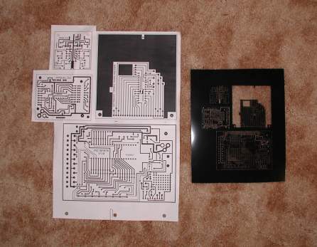
The artwork on left was taped together to produce one negative film on the right. This is the most economical way. You can cut the negative with scissors into separate negatives.
If you would like to see what the layout for a 16F84/628 prototyping board below will look like on your HP Laserjet printer, download this zip file. Unzip it and you will have two files. f84-1.prn and f84-2.prn. To print a 2X image, open a DOS prompt to where you unzipped the files and type [type f84-2.prn >lpt1]. Note this has to be printed from a local computer (non network) in DOS mode and not a USB computer.


3. Reducing to negative film. This step is not as hard as you may think. There are many places you can go to have the film made as shown in the picture (above right). In the small town I live in, there are at least five places that I can use. Just about any printer (print shop) can do the job. Even the local newspaper has a camera that will do the job. Make friends with the camera operator or owner. I usually like the smaller print shops because you can usually have a one on one relationship with the owner or camera operator and they can be very accommodating. What you need to do is ask for a "50 percent reduction to negative film (Kodaith Ortho or equivalent), emulsion side down". The camera is usually called a floor camera or vertical camera. Printers use these cameras to make all their negatives when printing books, flyers, business cards, advertisements, etc. (Although recently, most print shops are using computers for all their artwork generation and outputting right to the press machines.) If they are not real busy, sometimes you can wait for them to do the reduction and within fifteen minutes walk out with your negative. Other times you may have to pick it up the next day or drop it off in the morning and pick it up in the evening. The cost is nominal usually about US$8 to $12 for an 8X10 sheet of negative. This is usually the minimum price you will pay so you may want to tape a few small layouts together to make it cost effective. If it is a board that you may want to make many of, just print a bunch of them and tape them together like the one in the contact frame picture below.
Major update!!!!!!! As of 2013 just about all the print shops in our area and I'm sure all over the U.S. have gone digital and have shut down the photographic camera reduction method for the efficiency of direct-to-digital processes. Ortho film and chemicals are being eliminated and are scarce. In doing some research there are a few places that do silk screening and use the same film process. See Film History.
So how are hobbyists, experimenters and engineers making printed circuit boards? If you have the money and the time, you can use services such as http://www.expresspcb.com and http://www.pcbexpress.com. Obviously you have to wait about a month or so to get a few boards. You can get them faster but you have to pay a premium price.
There are "iron on" methods and heat transfer methods using http://www.pcbfx.com . Results can vary greatly. All the supplies can be purchased from http://www.mouser.com. I had poor success on some and fair results on others. You will also have to use a laminating machine to heat transfer or use an iron.
4a. Exposing the board. (Dry Film Method) This is a relatively new method using the Dry Film technique. I use commercially available dry film sensitized boards and chemicals available from Dalpro. You can laminate dry film to clean blank copper boards yourself but the price of dry film and the equipment to laminate is not cost effective if you don't make dozens of boards a week. Dalpro will sell you 12X12 sheets of 1oz in bulk which is the most economical for most hobbyists. In a subdued room with a yellow bug light or yellow plastic filter over fluorescent tube, carefully cut the board at least a half inch more around the outside of the board boarder using a paper shear as shown below. Expose the board under a #2 photoflood lamp for approximately eight to ten minutes as shown below. Leave the protective film on the board at this time. Make sure the emulsion side of the film is towards the board.
After exposing, remove the clear film from the board and discard. You should still do the following under the filtered light. Be careful not to touch or scrape the film at this stage. By this time you should have mixed the DFD (dry film developer) and DFS (dry film stripper) water soluble chemicals using the directions that came with the powder. In a metal or glass tray, submerse the board in about a half inch of DFD. Slosh the board around by rocking the tray back and forth. You can use a small very soft brush to help remove the soft resist by gently wiping the board. When it looks sufficiently clean and your board looks like it should, remove and wash the board in a sink being careful not to damage the hardened resist. Go to section 4c to see in detail the exposure method and skip section 5 and go to section 6.
4b. Exposing the board. (KPR Method) A photo sensitized copper board is required to make the circuit board. You can either sensitize your own boards or purchase pre-sensitized boards. To sensitize your own boards, you have to start with a copper clad board scrubbed clean. I use scouring powder and an old sponge. Let it dry without touching the surface, spray or wipe on the photo resist. Years ago I bought a quart of KPR (Kodak Photo Resist). I have made over a thousand boards and still have over half the bottle left. The resist does not become photosensitive until it dries. I use dust free makeup removing pads available from the drug store to spread the resist. Pour about a quarter sized amount of resist liquid on the dry board and wipe the board one way and then 90 degrees the other way. Handle the board by the edges and lean the board against a wall or other object in a very dim lit room, and lean it wet side down so dust doesn't accumulate on it. It doesn't have to be pitch black where you dry them, just dark enough for you to move about freely. You can make a number of these boards and keep them between the pages of a large thick telephone book separated by a few pages. Air doesn't seem to degrade the photo resist. I have sensitized boards as large as 16X20 inches with no problems.
I used to buy sensitized boards from Kepro. They came in 12" X12" sheets sealed in black plastic. Single sided 1 oz, 5 pack, G10, p/n S1-1212G, is about US$100. Unfortunately they are out of business.
When opening the material package and cutting, do so in a dim lit area. Be careful not to touch or scratch the outer surface. I use a paper cutter/trimmer (shear, see below) to cut the board to the size desired. Cut somewhat larger, to an extra 1/2 inch all the way around the final board dimension. You may want to shear the 12X12 piece so it will fit into the large book for easy access. It doesn't have to be sealed air tight. Just kept them out of normal light. I have had some feedback by prototypers that have had problems shearing boards with a paper cutter. It is not that hard. You must lift the blade and place the board, sensitized side up as far forward, close to the pivot point of the shear machine. Use firm pressure and push the handle towards the center, tight against the stationery blade. Shear about three inches at a time for longer boards. You may also have to "rotate" the board slightly in order to keep the cut straight. The shear will have a tendency to drift. Experiment on a few pieces of scrap board to get used to cutting. If cutting single sided photosensitive boards, always cut with the sensitized resist side up. If making long cuts tilt the right side of the cut portion under the pivot point of the shear. Take two to three inch cuts at a time. It will be necessary to place a piece of plastic electrical tape under the pivot point to keep it from scratching the resist. When cutting double sided sensitized boards, place a piece of paper on the cutting table top to keep the top from scratching the bottom resist.
4c. When placing the negative on the board, I usually take a small piece of "Scotch" magic tape and tape the negative on the board to keep it from shifting when placing on a contact frame. Remember that the emulsion side (dull side of the negative) should go towards the copper. This is another reason to have printing on the board so you can verify the direction of the negative.
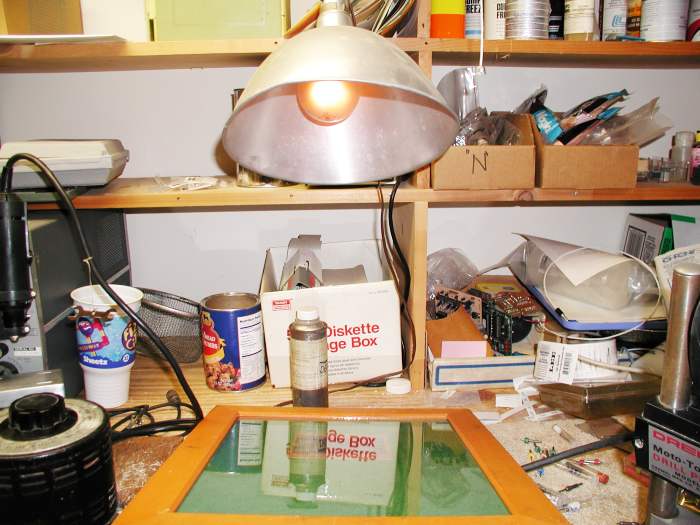
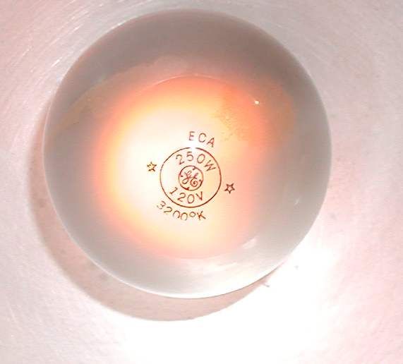
I use a Number 2 (250 watt) photoflood bulb in a flood light reflector and a 12X16 contact frame, both available from your local photographic dealer. Forget the fancy ultra violet tubes and exposure frame you have to make. The contact frame is simple and safe and will allow you to expose large or small boards at ease.
With everything going digital, frames might be a little hard to find and you may have to make one from a flat board and a piece of glass.
Suspend the bulb about 12 inches over the frame and expose for approximately 8 to 12 minutes. I use a lamp dimmer rheostat (shown above, far left) to bring up the brightness to full. This makes the bulb last longer but not really required.
Sometimes I will expose many small boards simultaneously in the frame at one time.
There are two basic ways to expose a double sided board. One way is to tape both boards together with a piece of circuit board material on one edge. This provides the necessary spacing and allows you to register the board sides together. The other way is to use tooling holes either inside or outside the board layout. Tooling (registration) holes are drilled in the board and are used to align the sides separately and exposed separately. A future demonstration of this process is in the making. See paragraph 10.
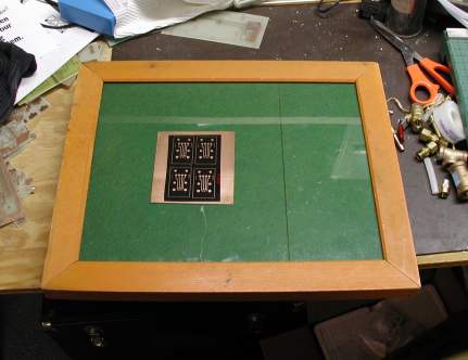
A contact frame with negative and board ready to expose
5. Developing the board. Once the board has been exposed, the portion of the board that had light on it will become hard and the developer will not remove it. Two chemicals can be used to develop the board. Xylol (Xylene) or Methylene Chloride. Xylol can be purchased at most hardware stores as a type of paint thinner/cleaner. Always perform the following in a well ventilated area and away from any open flame or space heaters. Remember that the board should not be exposed to normal light at this point. Use a glass or metal tray. Pour a small amount of developer in the tray and immerse the board copper side up. Gently agitate the developer by tilting the tray back and forth being careful not to spill the developer. Xylene is a little slow and it may take over 90 seconds to complete. Lift the board out and pour the developer into a separate container. DO NOT pour it back into your clean developer can. Tilt the board over the tray and pour a gentle stream over the board as a final wash. Do not shake the board dry. You should be able to see the resist in the form of your circuit at this time if you hold it up to the light correctly. Methylene Chloride may be a little harder to find but it works almost instantly and evaporates in just a few seconds. DO NOT INHALE these vapors or get too much on your fingers. Methylene Chloride can be purchased as liquid paint stripper at Lowe's.
If you are developing double sided boards, care must be taken not to have anything come in contact with the resist because it is very soft and will smear or wipe away. Use a metal clip that you can make yourself or a "bobby" pin clipped to one edge. This should keep the bottom side from coming in contact with the tray.
Sometimes you can just hold the board almost vertical over the tray and pour a stream over both surfaces to develop.
6. Etching the board. There are two chemicals used to etch the undesired copper away. Ferric Chloride and Ammonium Persulfate (or Sodium Persulfate). I used to use Ferric Chloride but it was messy, stained everything it came in contact with, hard to dispose of, and you can't easily see the etching process. Radio Shack may still sell it. I now use Sodium Persulfate. Both chemicals will etch faster when warmed. The Sodium Persulfate will work much faster when it is brought almost to a boil.
I use a glass casserole dish suspended above a hot plate. The glass must not come into contact with the hot plate or it will crack. I pour about two tablespoons of etching powder into about 3/4 inch of water. Add one drop of catalyst to the solution. Bring the water up to almost boiling temperature. Lay the board copper side down in the solution. The board seems to etch faster with the copper side down. I use a long narrow strip of circuit board material as a utensil to agitate the board and to lift it in and out. Don't be alarmed if the solution turns all kinds of muddy brown colors early on. It will soon turn clear again. Agitate the board until all the unwanted copper disappears. This will take only a few minutes. When done, remove the board and rinse in water and dry with a paper towel. You can use the solution maybe a second time or until the solution turns a pale blue like the color of Windex glass cleaner.
Dispose of spent solution accordingly. What does that mean? Don't ask. It's not that potent at this point anyhow.
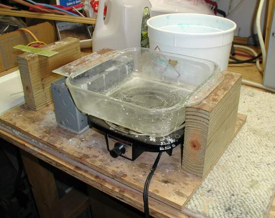
For smaller boards, I use a square dish with a metal box under one glass handle to support it. If I use a larger casserole dish, it will span across to both wood blocks. Remember to keep the dish from contacting the hot plate directly. Follow section 7a for dry film stripping and 7b for KPR method for stripping.
7a. Remove the resist. In a tray submerse the etched board in about a half inch of DFS and brush away any left over resist until clean. Thoroughly wash the board and dry with a paper towel.
7b. Remove the resist. I use an old rag and I wet a small portion of it with old developer and wipe the resist off the traces until clean.
8. Drill and shear. I use a Dremel Moto-Tool and associated drill stand. This is the best way of drilling circuit boards. I've heard of others trying to drill freehand or using a full size drill press. This is clumsy and inaccurate. Full size drill presses cannot achieve the speed in making a clean hole, and getting to the center of the pad is awkward.
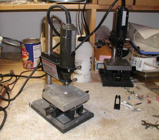
This drill press has lasted me over 25 years! I think I have only broke three bits in that time. My standby press in the background I got off of Ebay for about $60. This particular model is obsolete and what is currently available new doesn't work anywhere near as nice as this one.
Always use carbide drill bits. Regular HS (high speed) bits are totally useless. Two sizes of bits usually meet most of the hole size requirements. (.032 #67 and .052 #57) Carbide bits are very brittle and any slight side movement of the bit or board will snap them off. Be careful and make sure the bit comes out of the board before moving the board. The drill runs at 10,000 rpm. I use a variac to reduce the speed to about 5,000 rpm or less. Fast enough to drill all holes. No need to burn the drill up any faster than you have to. If you're careful, you can get over a year of use out of a carbide bit. I have one that I use all the time and has lasted over 6 years! Some bits are straight shank and some are tapered solid shank. Either will work equally well. Below are mostly tapered shank bits.
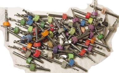
Sometimes you can buy a bunch of them in various sizes on Ebay
or from Yahoo
Shopping.
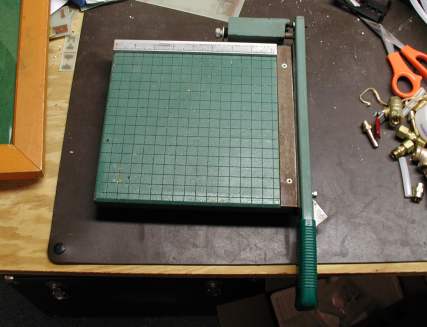
This paper trimmer is made by Premier (Search Staples.com or Officemax.com if these links don't work). After thousands of board cuts, I can still slice a single piece of paper. Look for one that has a good solid stationery pivot point like the one pictured in the upper right corner of the unit. There are some real cheap models that won't survive the cutting process and may break. Mine cost about $40.00 when I bought it years ago.
I use the paper trimmer to shear the board as close to the board dimensions as I can. I then use a small combination belt/disc sander to give it a smooth clean square edge. Use a dust mask and/or sand the edges outdoors where the dust dissipates. Forget about using a hack saws, band saws, Dremel disc cutters, metal shears, circular saws, jig saws, tile cutters, or coping saw. They create too much dust, and don't make a good straight cut. A corner nipper or nibblers can cut any oddball dimensions required. A file can clean the inside corners of the board if required.
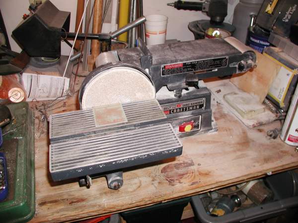
Disc sanders like this can be purchased for around US$37.99 from Harbor Freight or Sears. Use outside or in a well ventilated area, and/or wear a dust mask.
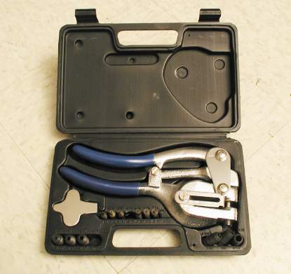
A punch tool is great for punching quick, clean holes 3/32, 1/8, 5/32, 3/16, 7/32, 1/4, 9/32 excellent for screw holes, nylon standoffs, mounting larger components to board. Drilling large holes leaves rough unclean holes and sometimes punching through the board will cause the board to lift and get away from you. This tool available for about US$16.99 from Harbor Freight.
9. Tin plating. Electroless tin plating solution can put that finishing touch on the board but I never had the need to. Here are some old boards that I have made and the copper has not tarnished or oxidized.
10. Making double sided printed circuit boards. I am in the process of taking pictures and will soon have a complete procedure for making simple double sided circuit boards. Rick - 12/03
Off Topic
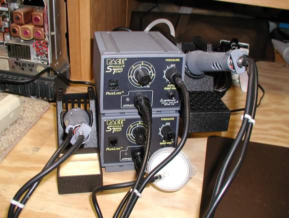
I picked up this fancy hot air soldering/desoldering station
for less than US$100 new in box at a Hamfest!
This particular model happens to require 80 PSI pressure and 230 volts. My shop compressor
provides the power and a step up transformer from Jameco
converted my 117 volts to 230 volts.
An excellent tool for surface mount soldering and thru-hole parts removal.
Sometimes you can pick up items like this at a "hamfest".
Text and pictures Copyright © 2014 by Rick C.
Many of the links on this page are specific. If you find the link broken, it may mean they have changed its location. Go to their root site and do a search. Please notify me if this is the case.
Any questions or comments can be directed to Rick.
This site has been providing free information for over ten years. We ask for no monetary remuneration. However the cost of keeping this domain and server running has increased substantially. If you are so inclined, you can make a donation no matter how small to keep this site always available. You can click on the Paypal button to donate. You don't need a Paypal account to contribute. Thanks for your support.